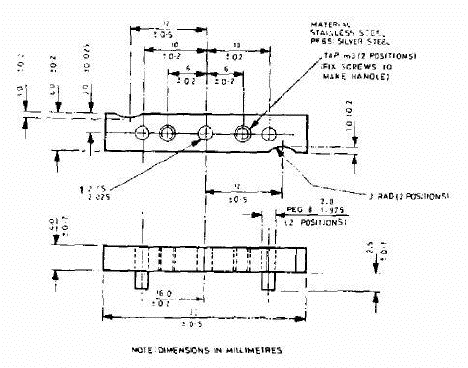
FIGURE 4.1 MOTOR LOCATION JIG
| Sinclair QL Service Manual | ||
|---|---|---|
| Previous | Next | |
1.1.1 Section 4 is intended as a guide to fault diagnosis and repair. It is assumed that users have a reasonable knowledge of electronic servicing, theory and standard fault-finding techniques and have access to the test equipment and tools required to carry out the task. The table below contains a list of the minimum test equipment and materials.
| EQUIPMENT | SPECIFICATION/MANUFACTURER |
|---|---|
| Oscilloscope with probe (x1O) | Rise time: 0.02 µs/cm |
| Multimeter | General purpose |
| Colour Television | Open market |
| New microdrive cartridges | as required, Sinclair |
| Head cleaner | Open market |
| Double-sided adhesive tape | Open market |
| Extension ribbon/connectors for J11, J12 and front panel LED wiring (to enable operation with cover off) | Make up on site |
| ZX Microdrive | Sinclair |
| Motor location jig | See Figure 4.1 |
1.1.2 See Section 5 for the board layouts of the Issue 5 and Issue 6 boards.
FIGURE 4.1 MOTOR LOCATION JIG
1.2.1 The only area that has seen substantive modification is the ROM/EPROM section of the memory. The following table sets out the various fits.
| Build Standard | IC | ROM/EPROM | Software Standard | Remarks | |
|---|---|---|---|---|---|
| ROM | EPROM | ||||
| D6 | IC33 | - | 32k | AH | 16k of EPROM mounted pickaback on IC33 |
| IC34 | - | 16k | |||
| D7 | IC33 | - | 32k | JM | 16k of EPROM mounted pickaback on IC33 |
| IC34 | - | 16k | |||
| D8 | IC33 | 32k | - | AH | |
| IC34 | - | 15k | |||
| D9 | IC33 | 32k | - | AH | |
| IC34 | 16k | - | |||
| D10 | IC33 | - | 32k | JM | |
| IC34 | - | 16k | |||
| D11-D14 | IC33 | 32k | - | JM | |
| IC34 | 16k | - | |||
1.2.2 A newly laid out p.c. board was introduced at Issue 6 to reflect the removal of IC17 and IC27 and the addition of HAL IC38. Resistors R102, R103 and R104 were added at this stage and trimming capacitor TC1 was replaced with a fixed capacitor C53 of 22pF. The parts list reflects minor changes to component values. Board layouts are shown in Figures 5.1 and 5.2.
Certain component modifications have been introduced to improve performance in specific areas. These components should be checked for on all units coming in for repair, and if necessary, fitted as a matter of course. These components are listed below:
2.1.1 In a closed loop system such as a computer, because of the interdependance of numerous component parts, fault diagnosis is not necessarily straight-forward. In addition, because of the high speed cyclic operation, interpretation of any waveforms on control, data and address lines as being valid depends to a large extent on practical experience of the system. There are however, certain checks with valid waveforms and levels that can be carried out before substituting any integrated circuits. Experience has shown that the best method of initially checking waveforms and levels can be to compare with the same point in a known serviceable board. The following pages provide a basic fault-finding procedure and furnish a list of possible faults along with suggested ways of curing them.
2.1.2 With a densely populated board such as in the Sinclair QL, a careful physical examination of the board can sometimes indicate an obvious fault. Burst-out discrete components or an overheated track show up immediately, as do the attentions of an enthusiastic amateur. Bearing in mind the latter, short circuits caused by hairline solder 'splatter' can be of several ohms resistance and can cause some very misleading fault symptoms.
2.1.3 It may be that the label on the faulty unit setting out the customer's assessment of the fault is unreliable. It is therefore usually best to approach the repair task with an open mind and start the diagnosis with no pre-conceived idea of the fault.
2.1.4 Where the substitution method is used to check a suspect component, the suspect component should be connected into the known serviceable unit rather than the other way around. The faulty component is less likely to damage the working unit, thus safeguarding the unit and the known serviceable component.
2.1.5 Provided first principles are adhered to and a common-sense approach is adopted, it will be found after a short space of time that fixing a faulty QL is very much a routine operation.
NOTE: It may be advantageous to operate the QL with the cover removed, using extension connectors (see para 1.1.1).
2.2.1 At switch-on, the yellow power indicator illuminates and the QL should automatically power-up and produce a clear screen with the following displayed at the bottom centre of the screen:
F1...MONITOR
F2...TELEVISION
© 1983 Sinclair Research Ltd
2.2.2 This indicates that most of the system is working. If the QL does not power up, and display the expected copyright screen, switch off and repeat the power-up operation two or three times. It is possible for the QL to lock-up on start-up and appear lifeless.
2.2.3 Lack of a copyright screen indicates a fundamental failure. First check voltages as set out in the table below.
| FUNCTION | CIRCUIT REF | WAVEFORM/VOLTAGE |
|---|---|---|
| ± 12 V voltage regulator input | + side of D26 | 15.6 V a.c. ± 2.0 V |
| + 5 V voltage regulator input | + side of C41 | + 9.0 V a.c. ± 2.0 V |
| + 12 V voltage regulator output | FT side of C38 | + 12.0 V d.c. ± 0.25 V (no discernible ripple) |
| + 5 V voltage regulator output | FT side of C42 | + 5.0 V ± 0.15 V (no discernible ripple) |
2.2.4 The state of the display screen provides a good indication of the possible fault. Three general categories of fault display may be isolated.
2.2.5 A completely blank screen on switch-on is often caused by a faulty IC22 (8301). Since this is a plug-in component it can easily be substituted. If this does not cure the problem, suspect a video fault and if it has not already been done, plug in both a monitor and a TV and check for video output. If a replacement IC22 is not available, check that the clock signal to the CPU, and the RGB output signals are present.
2.2.6 If the RAM test is seen to be starting up before the system crashes, it means that the 8301 is working and that the ROM is being read and the program is starting to be executed correctly. The start of the RAM test is indicated by the display of a fine pattern , of green, white, red and black dots (tweed pattern) which move quickly down the screen and disappear. Fault-finding would start with the RAMs in this instance.
2.2.7 If the screen displays a geometric pattern (for example, red and green vertical bars), it means that the 8301 is working properly but is not actually starting to execute the ROM code, it is not overwritng the RAM data. It is possible that the 8301 clock to the CPU is missing, or again that RAM is faulty. An absent CPU can also give the same effect.
2.2.8 If the machine reaches the end of the RAM test, displays a geometric pattern and then reverts to a blank screen it could mean any one of the following:
2.2.9 If the ROM enable signal (pin 33, 8301) is not present, the ROM is unable to excute correct code. If, on switch-on, random flickering patterns are displayed, accompanied by excited beeping noises this suggests a faulty ROM. If the ROM is functioning but the RAM is not, then the screen displays a white or green screen. This testifies that there is something wrong with the RAM.
2.2.10 The RAM test is divided into two parts, the first where it checks that it is possible to store ones, zeros and random pattern in every RAM location, and the second part a few seconds later when it checks that the stored data is still there. A white screen means that the first part of the test has failed and a green screen means that the second part has failed.
2.2.11 A green screen can mean either that memory is not being refreshed or that there is a possible short in one of the address or data lines causing mis-routing of a bit of data. Check visually for shortcircuits across pins or address data lines in the, RAM area itself and then further afield (e.g. at the CPU). It may then be necessary to carry out checks using an ohmmeter. Bear in mind that it is possible to obtain misleading readings when, for example, the meter is feeding back through the CPU.
2.2.12 If the screen is not quite pure white or green and has either very narrow vertical stripes, or a vertical pattern of dots, this indicates that one bit in the system is faulty, either as a result of a fault within one of the RAM chips or of a short-circuit across a data/address line. In order to pin-point the faulty RAM chip, proceed as follows:
2.2.13 If RESET is pressed and a 'tweed' pattern is seen on the screen for a certain time and it then reverts to white, this suggests that some failure has been found in the second bank of RAM.
2.2.14 To summarise, if on power up a white or green screen is displayed, it indicates that the RAMs are in general working, and that the machine is very close to being fully operational. It suggests a data or address line short-circuit or a faulty RAM chip.
2.2.15 If it is plain that the machine has not really started performing the RAM check at all, check for the regular occurrence of the DTACK signal (pin 31, CPU). If this is not present the RAM test can never be initiated. Check for a short-circuit on the DTACK line and check the 8301, particularly the DSMCL signal. A high level on the latter disables the 8301.
2.2.16 Where uncertainty exists as to the best place to start fault finding, carry out the following checks by comparing with a known good board:
| IC23 | Pin 32 - VSYNCH Pin 10 - PCENL Pin 8 - DCSML | Pin 28 - RESETOUTL Pins 30, 31 - XTAL Pin 25 - CLOCK |
| IC18 | Pin 21 - DTACK Pin 30 - R/W Pin 29 - DS | D0-D7 - Data Lines A0-A17 - Address Lines |
| IC22 | Pin 38 - VDA Pin 37 - ROWL Pin 33 - ROMOEH Pin 9 - CASOL Pin 8 - RASL Pin 40 - WEL Pin 10 - CASIL | Pin 36 - TXOEL Pin 4 - RDWL Pin 12 - CSYNCL Pin 30 - RED Pin 31 - GREEN Pin 32 - BLUE Pin 7 - CLOCK |
2.2.17 When the fault persists it may be necessary to start changing individual plug-in ICs, in the order IC18, IC22, IC23, IC24 and IC28. After each change of IC the unit must be powered up to check for correct initialisation.
2.2.18 A method of fault-finding that might be of use in checking non plug-in ICs is to use a 'test IC' device. This can be made up using an IC test clip, to which is attached a serviceable IC (of the relevant type for example 4164 for RAM) to bridge across each suspect IC in turn. This method is not guaranteed to work but can often save a lot of time unecessarily changing suspect ICs.
2.3.1 The keyboard is connected as shown in Figure 4.2. The configuration is basically an 8 by 8 matrix with partial extra diode isolation. From an examination of the faulty keys it should be possible to isolate a faulty membrane or circuit component. Possible keyboard faults are listed in paragraph 2.6.
2.3.2 Apparent major keyboard problems could be associated with the 8302 or the IPC itself but more commonly faults are likely to be on the membrane or the connectors. If a given row or column does not respond, the fault can be narrowed down to one of the connectors. If a pair of keys is faulty it could be that there is a short-circuit between them. Again, it is possible that two rows might not be working, indicating a short-circuit. Check for these with the ohmmeter.
2.3.3 To see what is happening on the keyboard, connect a double-beam oscilloscope, and trigger from one of the keyboard outputs (e.g. KBO1). Check that all the other outputs are going high at successive intervals. The effects of a short-circuit affect the timing of the scan pulses and can easily be seen.
2.3.4 A common fault is a break in the keyboard membrane. If the break is close to the connector it is possible to remove the ribbon from the connector, slice off a short section above the break and plug it back in again. If the break is elsewhere a new membrane is required. The main objective in this area is to establish whether the fault is on the membrane or the board.
2.4.1 The microdrives have been a source of some problems in the pre-lssue 6 units. The mechanical layout is shown in Figure 4.3. Mote that it is not possible to replace the read/write head on the microdrives, but all other components are replaceable. If the system test indicates a microdrive failure, the indicated microdrive, MDV1 or MDV2, must be further investigated. Where the fault finding guide (para 2.4) indicates microdrive failure, refer back to this paragraph.
2.4.2 Establish that on-board voltages are correct by carrying out the checks set out in the table below. Circuit references are for MDV1 (with MDV2 references in brackets).
| VOLTAGE | CIRCUIT REF. | VOLTAGE VALUE |
|---|---|---|
| + 5 V | IC30 (IC29) pin 11, 7, 9 | + 5 V d.c. ± 0.25 V (no discernible ripple) |
| + 9 V | Pin 6 (6) of ribbon connector | + 9 V |
2.4.3 Microdrive problems can be conveniently split into mechanical and electrical faults. Some typical faults in both categories are listed in para 2.4.6 below.
2.4.4 If it is not possible to load from either microdrive, load MDV1 with a known serviceable pre-recorded tape and key in the following program:
100 DEFine PROCedure sedes(n,flag)

110 reg=98336:pc_sel=2+flag

120 FOR i=1 TO n

130 POKE reg,pc_sel

140 pc_sel=pc_sel&&253

150 POKE reg,pc_sel

160 pc_sel=2

170 END FOR i

180 END DEFine

200 DEFine PROCedure start_mdv(n)

210 sedes n,1

220 END DEFine

300 DEFine PROCedure stop_all

310 sedes 8,0

320 END DEFine
Key-in start_mdv(n) to turn on drive number n and to keep it spinning continuously. Key-in stop_all to stop all drives spinning.
2.4.5 An alternative method is to use a known serviceable ZX microdrive plugged into the microdrive expansion port. This isolates faults to either the machine or the microdrives.
2.4.6 Load and run the system test tape. Section 3, System Test, provides details on how to load this test. The following table lists possible faults and remedies. Where it is necessary to change or adjust the position of the motor, the motor jig (Figure 4.1) must be used.
| SYMPTOM | REMEDY |
|---|---|
| Screen displays 'Put a blank tape in MDV1 (MDV2)' even when tape present |
|
| Screen displays 'Failed microdrive test' |
|
| Microdrive does not operate when selected. |
|
| Tight cartridge tape. |
|
| Noisy operation. Fails to format. Jammed tape. Damaged cartridges. Microdrive incompatibility. |
NOTE: If motor has over-heated, check for buckled baseplate. Renew complete microdrive unit. |
| |
| Head failure. | Renew complete microdrive unit. |
| LED failure. | Renew LED (LED is push-fitted). |
| Check mod state (see Section 4, para 1.2.2) | |
| Unreliable loading/saving, machine locking-up. |
|
| Continuous running MDV1(MDV2). | Renew TR7(TR6) |
| MDVs do not activate. | Renew IC23. |
| Erase function not working. |
|
| MDV1(2) does not run | Check TR7(TR6), TR5(TR4) |
2.5.1 Video faults are either total, when there is absence of monitor and TV signal, or may be categorised as either monitor or TV faults.
2.5.2 If a TV is initially connected and is giving no picture it might be worth tuning the set slighly either side of the expected tuning point. (It is possible the modulator has drifted slightly). If a picture is displayed but without colour, use the oscilloscope to check that crystal X3 is actually oscillating. Look at the video output and check for colour modulation on top of the luminance signal. If it appears that chrominance and luminance are present at the video output but the TV does not give colour, it probably means that the crystal frequency is wrong and the TV cannot lock on to it properly. If no chroma is present then the chroma oscillator is not oscillating. If the chroma is present and there is no TV colour it is possible that changing slightly the value of C31 may be sufficient to bring back the colour. Check, using a monitor or by looking at the signals that RGB inputs are present. If they are, consider changing IC28, and checking the circuitry around it.
2.5.3 It is possible that the modulator is faulty. This is checked by removing IC28 and feeding the VIDEO signal (from TR9) in via R85. This gives a rather low contrast signal in black and white only.
2.6.1 The following table is not intended to be an exhaustive list of the faults that might occur on the Sinclair QL. It is intended as a guide only to possible courses of action to follow when faults show up in particular areas of the circuit. These areas are listed in the table with sub-headings, in no particular order of priority. It is envisaged that the system test has been loaded, or an attempt has been made to load it, in order to check for a faulty condition.
| AREA | SYMPTOM | ACTION |
|---|---|---|
| Screen | TV/monitor screens black. Power light on. Fails to power-up. | Check voltages (para 2.2.3) Renew IC22 Renew IC24 Check RAMs Renew IC34 Renew IC18 Renew IC33 |
| Power | PSU noisy. | Change PSU |
| Loss of power. | Check IC37, IC36 | |
| Display | Erratic display after warm-up period. | Check RAMs. |
| No colour TV output. | Check C35, C36, R85, R86. Check C29, R54 and components around IC28. Renew modulator M1. Renew IC28. | |
| Dark TV screen. | Renew modulator M1. | |
| No B/W TV output. | Renew TR9. | |
| No colour monitor output. | Renew IC22. | |
| Fails colour test. Colour loss/fades. | Renew crystal X3. Check components around IC28. Renew IC28. | |
| TV output distorted. No TV output. | Renew IC35. | |
| Blurred vision. | Renew IC22. | |
| TV picture drifting continuously. | Check C23, C24, C25. | |
| TV/monitor picture drifting. Gradual loss of colour in use. | Renew IC22. | |
| Keyboard | Fails keyboard test: | |
| Keyboard does not respond. | Check connectors J11, J12. Check ribbon cable. | |
| Multi-character printing. Keyboard bounce. Keys sticking down. Key(s) does not register. | Renew membrane. | |
| Key(s) does not always register. | Renew bubble mat. | |
| 'Sticky' key(s). | Clean key surfaces. Renew bubble mat. | |
| Continues to fail keyboard test. | Renew IC24 Renew IC18 | |
| Keyboard locks-up after prolonged use. | Renew IC23 Renew IC24 Renew IC18 | |
| RS232-C/Printer | Fails RS232 loopback test. | Check J5, J6 Renew IC25, IC26 Renew IC23 Renew IC24 |
| Network | Fails network test. | Check J9, J10 Check TR2 and associated components. |
| Sound | Fails sound test: | |
| No sound | Check TR1 Check R104 (post-Issue 6) Renew IC24 | |
| Real-time clock | Fails real-time clock test | Check R91, R80, C1, C53. |
| Joystick | Fails joystick test. | Check J3, J4, J2 |
| Fails reset test | Does not reset. | Check reset switch. Check reset switch spring. |
| General | System locks up after prolonged use. Computer 'crashes' at random intervals or after prolonged use. | Renew crystal X2. Renew IC23 Renew IC34 Renew IC24 |
3.1 Renewal of components should be carried out using recognised desoldering/heatsinking techniques to prevent damage to the component or to the printed circuit board. Other points to be noted are listed below:
When replacing a keyboard matrix, take care that the ribbon connectors are fully inserted into the board connectors, and are not kinked during insertion.
Make sure there is a good contact made between the voltage regulator (IC35) body and the associated heatsink in order to ensure adequate heat conduction.
When regulator IC35 is being renewed it is recommended that a suitable proprietary thermal grease is applied to the rear surface of the component body.
The modulator should be renewed as a complete unit.
When renewing/replacing plug-in ICs it is advisable to use the correct removal and insertion tools. Avoid contaminating the connection pins by handling.
When handling ICs take normal anti-static precautions. It is recommended that only a suitably earthed, low power soldering iron be used.
4.1 It is often obvious that an upgrade is required by the presence of a pickaback device in position IC33. However, in all instances, refer to the build standard and serial number found on a label stuck to the bottom of the case, e.g. D09 123456. Prefix D09 refers to the build standard and 123456 gives the serial number. All units to build standards D8 and below, plus D10, must be upgraded to D11 or later firmware.
4.2 The materials for the upgrade are:
4.3 The upgrade is carried out as follows:
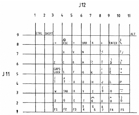
FIGURE 4.2 KEYBOARD FORMAT
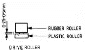
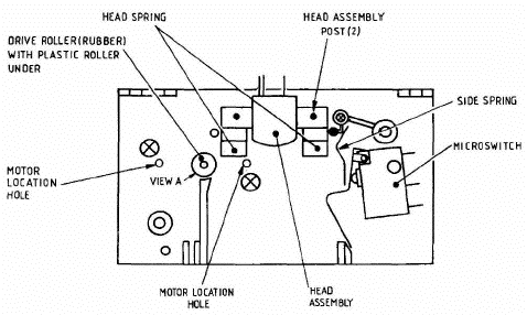
FIGURE 4.3 HEAD CHASSIS
1.1 You may have been experiencing difficulty in getting an adequate performance from a monitor connected to your QL. Given below is a revised set of wiring instructions for the connection lead. These instructions replace those given in page 31 in the Concepts section of the QL User Guide.
1.2 Monitor Connections. A monitor may be connected to the QL via the RGB socket on the back of the computer. Connection is via an 8-way DIN plug plus cable for colour monitors, or a 3-way DIN plug plus cable for monochrome. The RGB socket connections are as in the following table, and the column indicating wire colour refers to the colour coding used on the 8-way cable and connector available from Sinclair Research Ltd. Pin designation is as shown in the diagram attached.
1.3 A monochrome monitor can be connected using a screened lead with a 3-way or an 8-way DIN plug at the QL end. Only pins 2 (ground) and 3 (composite video) need to be connected via the cable to the monitor. The connection at the monitor end varies according to the monitor but is usually a phono plug. The monitor must have a 75 ohm 1V pk-pk composite video non-inverting input (which is the industry standard). Both 3-way DIN plugs and phono plugs are commonly available from audio shops.
1.4 An RGB (colour) monitor can be connected using a lead with an 8-way DIN plug at the QL end. The connection at the monitor end varies according to the monitor (there is no industry standard) and is often supplied with it. A suitable cable with an 8-way DIN plug at one end and bare wires at the other end is available from Sinclair Research Ltd.
1.5 A composite PAL monitor, or the composite video input on some VCRs may work with the QL. Only pins 2 (ground) and 1 (composite PAL) need to be connected via a cable, to the monitor or VCR.
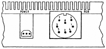
Diagram of Monitor Connection Viewed from the Rear of the QL
| Pin | Function | Signal | Wire Colour | Signal Level |
|---|---|---|---|---|
| 1 | PAL | Composite PAL | Orange | 1V pk-pk into 75 ohm |
| 2 | GND | Ground | Green | |
| 3 | VIDEO | Composite Mono Video | Brown | 1V pk-pk into 75 ohm |
| 4 | CSYNC | Composite Sync | Yellow | 0 to 5V TTL (active low) |
| 5 | VSYNC | Vertical Sync | Blue | 0 to 5V TTL (active high) |
| 6 | GREEN | Green | Red | 0 to 5V TTL (active high) |
| 7 | RED | Red | White | 0 to 5V TTL (active high) |
| 8 | BLUE | Blue | Purple | 0 to 5V TTL (active high) |
2.1 There are a number of bugs still alive in the QL. Some are rather obscure, but here is a list of the ones that could cause a customer to return a QL as "faulty", together with the clue you should look for when you suspect a bug is the real problem.
If you delete a procedure which was at the end of a program and then call the same procedure from the keyboard, and then call CLEAR, the QL may crash.
Clue: Computer crashes after CLEAR command.
"LIST" within a program can cause various unfortunate states, e.g. "not implemented".
Clue: "LIST" within a program.
The command "CURSOR #n, a, b, c, d" is not accepted.
Clue: "CURSOR #n, a, b, c, d" gives "bad parameter" (NB: message "channel not open" is NOT a bug).
If an expression in a DATA statement starts with a bracket [(], the rest of the DATA line is ignored.
Clue: DATA ...., ( ...),
GOSUB in short FOR loops can act as ENDFOR.
Clue: GOSUB in a short FOR loop.
If you ask for DIR mdv8_, then DIR mdv2_ will not work properly thereafter.
Clue: DIR mdv8_
NOTE: A bad microdrive 2 can cause the same symptoms, so beware!
If a program aborts in the middle of a PROCedure, and you type EDIT, you get "not implemented", and you are left editing a spurious line number.
Clue: EDITing PROCedures.
Sometimes variable names get over-written by the word "PRINT". This is random, so far as we know.
Clue: "PRINT" in unexpected places.
If you declare more than 9 local variables, all sorts of unexpected things can come up on the screen.
Clue: LOCal a, b, c, d, e, f, g, h, i, j, ...
Note that if the "fault" can be repeatedly demonstrated on the customer's QL, but not on another one with the same RDM version, then it is not a bug.
If the fault cannot be reproduced at all on the customer's QL, then it MAY be a random bug (e.g. item (h) above), but this is most unlikely.
2.2 In some circumstances, the use of slices of strings leads to memory being allocated which cannot be reclaimed without the use of CLEAR. Either of these will run out of memory eventually:
10 DIM a$(10,10)

20 a$(5) = "hello"

30 REPeat x: PRINT a$(5, 1 TO 4)
or
30 REPeat x: PRINT a$(5)(1 TO 4)
2.3 CLEAR, LOAD or NEW are the only ways of getting this memory back; these commands delete all the variables. (Remember that RUN on its own leaves variables untouched - put a CLEAR and/or restore at the start of your program if you need to). To avoid this problem, use:
30 REPeat x: temp$=a$(5): PRINT temp$(1 TO 4)
This problem only arises with string arrays, not with numerical ones.
2.4 One bug has inadvertently been introduced into the QL with the introduction of the JS ROM. in a procedure, if you SELect ON one of the parameters of the procedure, you get "bad name", unless you are SELecting ON the last one.
i.e.
DEF PROCedure f(x,y)
...
SELect ON x gives "bad name"
SELect ON y is OK.
This bug is only present in the JS ROM. You should also note that you cannot SELect ON a character string.
2.5 Another obscure bug on the QL is as follows. If you ever open the SER2 port, either by an explicit OPEN command, or indirectly by LOAD, COPY, SAVE etc, please note that the channel can never be properly closed again, even using the CLOSE command. In fact CLOSE (SER2) closes SER2 output and SER1 input.
2.6 One effect of this is that if you subsequently input data via SER1, and you have a device that is also trying to send to SER2, the data streams will get muddled. One way round the problem is to unplug the lead from SER2 when not in use. This bug is present on all current versions of ROM (AH, JM and JS).
3.1 If a customer complains that his printer will not print more than about a page of output from his QL, he should check the wiring in the lead.
3.2 Many printers require the DTR line to be connected to pin 20. Some of these, by chance, work with the DTR line connected to pin 4, until one buffer full of data is printed.
3.3 If the problem does occur, look at the wiring of the RS-232 lead on the end that connects to the printer, and check that a lead exists, connected from pin 4 to pin 20.
4.1 There is one potential fault with the SER outputs from the QL that is not obvious to find.
4.2 If either pin 1 (ground) or pin 6 (+12V) is not properly connected (e.g. lead not soldered to pcb), on either SER1 or SER2, the port may work, although any device that draws power from the QL, (e.g. a serial-to-parallel converter) would not operate.
4.3 Apart from checking visually, one test would be to connect pins 1 and 6 externally and check that 15 mA to 20 mA of current flows.
5.1 You may have a QL that "freezes" after a few hours of operation. We do not yet fully understand why this happens with some computers.
5.2 To cure the problem, take out all the ICs that plug into sockets, in the main pcb. Using some proprietary cleaning fluid, clean the legs of the ICs, and the sockets; then replace the ICs. In most instances, this cures the fault.
6.1 Run the following program to demonstrate an annoying screen flicker.
10 BLOCK 40,40,40,40,20

20 GO TO 10
This is common to all QLs, and all versions of ROM.
6.2 You can also see the effect if you move window 0 to put the cursor near the top left-hand corner of the screen. In this position the cursor has not had time to refresh itself before the screen refresh reaches it.
The following points may be of help in spotting 'non-faults' on QLs.
Please note that if you want the QL to tell you which version of ROM it has, you should enter 'PRINT VER$' and not 'PRINT VERS'.
If you try to run Abacus, Archive, Easel or Quill on microdrive 2 instead of microdrive 1, you get an error message, typically 'AT END 200 NOT FOUND'.
When saving data on microdrive 2 while using Abacus, etc., remember to use a formatted cartridge in microdrive 2 otherwise you get the message 'CANNOT OPEN FILE'.
If you have opened a data file when using Archive, remember to close it before removing the cartridge, otherwise future access may be difficult.
If you press the SHIFT key at the same time as the space bar, nothing happens when you are using Super Basic.
1.1 Refer to the mandatory modifications described on page 4.3 and page 5.1 in this manual. To check that if these modifications have been made, look for R102 and R103 through the SER1 port. If these resistors are in place you can assume that the other modifications have been carried out. With build state D12 or higher the modifications have already been incorporated.
2.1 On any QL requiring repair, it is recommended that the following modification be automatically carried out at the same time. On Issue 5 boards, cut the +5V track in position A on the component side of the board and in position B on the solder side. Then connect two links as shown in positions C and D. (See Figures C1 and C2). On Issue 6 boards, both track cuts are on the solder side. (See Figure C3). All current production incorporates this modification, which is identified by serial number D16 or higher, or modification label A4 or higher.
3.1 On any QL for repair, fit a special collar beneath the far right fixing screw of MDV2 (the screw by the side spring). This is to prevent the lid of the QL from hitting the top of the MDV2 board, which can upset the position of the head. Use a countersunk screw in place of the original one. Collars are available from Sinclair's normal spares distribution channels.
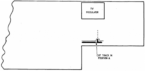
FIGURE C1 ISSUE 5 BOARD - COMPONENT SIDE (SRL/EI/1118-1)
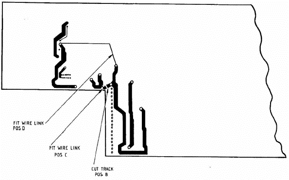
FIGURE C2 ISSUE 5 BOARD - SOLDER SIDE (SRL/EI/1118-2)
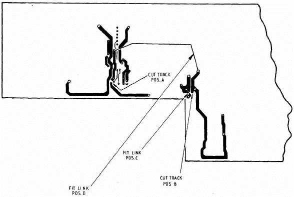
FIGURE C3 ISSUE 6 BOARD - SOLDER SIDE (SRL/EI/1119-1)
1.1 This guide is intended to give a base of understanding for the most frequent faults occurring on QL microdrives. It contains descriptions of faults and tests to help in finding them.
1.2 The microdrive is a slave mechanism for transferring data to and from magnetic tape. Its role therefore is not interpreting data, but ensuring that data presented to it for writing is read and returned in the same manner.
1.3 Before tackling signal testing, it is recommended that a mechanical check is carried out as detailed in Sub-Section 2, as this can save time, depending on the fault.
1.4 The program 'SIGNAL TEST' sends 100kHz to a microdrive in write mode, (erasing simultaneously) then puts it in read mode so that signals returned can be observed. This enables the performance of electronics and mechanics to be assessed with a steady waveform on an oscilloscope.
1.5 A two channel oscilloscope is required, as this can be set for measurement of differential signal nodes by adding CH1 and CH2 and inverting CH2.
2.1 Mechanical faults can adversely affect readability of tapes and subtleties, if not appreciated, can lead to a 'witch hunt' for a fault. The following exercises help, though it must be stressed that the mechanics are inter-dependent, so over-adjustment of one aspect may affect another. The effects of mechanical faults can be seen by using the signal test program as for read faults.
2.2 Roller: The motor drive roller should not be distorted in any way and should have the specified gap between it and the collar beneath it.
2.3 Motor Position: If not correct, this can cause tape slipping and speed problems. If these problems exist, check position using the appropriate jig.
2.4 Side Spring: With the tape spinning in the drive, push the cartridge away from the roller, depressing the spring. When released, the cartridge should return and spin freely against the roller without slipping or jitter. The top of the spring should be reasonably level and it should not foul the chassis.
2.5 Head Position: The digital head should have both front feet and at least one rear foot touching the chassis. It is not always possible for the other foot to touch due to head manufacture adjustments. If the head is tilted up, down or sideways, it will compound the'effects described for head spring. The face of the head should be clean.
2.6 Head Springs: Poor compatibility can be caused if this is weak or distorted. Looking from the front of the drive, the top of the springs should appear about level with the bottom of the lower head guides.
2.7 The effect of the springs can be checked using the signal test program as in sub-section 3 below. A tape should be written to and the pk-pk level noted when reading. This level should be reasonably attainable after the cartridge has been twisted clockwise and released and then anti-clockwise and released. There is a problem if the level drops significantly after settling for 7 seconds, in either direction.
3.1 To use the 'signal test' program (Table D1) proceed as follows:
Load the program into the QL and remove the program cartridge. A known good blank cartridge should be inserted into the drive to be tested.
The program asks which drive is to be analysed and when this has been entered, 100kHz is written to the cartridge in that drive for 8 seconds. The QL then 'beeps' and the drive is then 'reading' the cartridge.
Pressing the SPACE BAR stops and starts the process.
3.2.1 When 'signal test' is writing to tape, check that TTL data lines ULA pins 19 (24) are correct, as fig D1. If so, look at pins 4 and 5 (14 and 15) and compare to fig D2. If the signal is not present it is due to a faulty ULA or head.
3.3.1 After writing to tape, carry out the following while in read mode.
Check data lines ULA pins 19 (24) and compare to fig D3. If the waveform is very unstable in X axis, a mechanical fault is probable. If the waveform is poor or is not present at all check the pk-pk signal at pins 4 and 5 (14 and 15). See fig D4.
If the signal is present and correct there is a fault in the intermediate read stages. See circuit and fig D5. If the signal is not present at all and the write check is correct, then the head is faulty.
A low voltage at this point, due to a worn head, however can cause soft errors to occur when reading (e.g. 150 mV pk-pk).
If the waveform is very unstable in the Y axis (greatly differing pk-pk levels) the erase function is suspect. (This effect can also be caused by a poor tape).
3.4.1 This may be found to be necessary from the write and read checks. The effect described is due to residual magnetism in the tape from previous recordings not being erased when recording.
3.4.2 The microswitch is usually the culprit and can be checked for operation with power removed using a multimeter. To check erase using 'signal test' program, measure the following voltages:
during write/erase cycle:
| HBC, Pin 11: | Non Write Protected 5.6V Approx. |
| Write Protected 0.8V Approx. |
during read:
| HBC, Pin 11: | Non Write Protected 9.0V Approx. |
| Write Protected 0.1V Approx. |
4.1 Two faults are described below which may be present on some earlier microdrive ULAs but have since been remedied:
Pin 1 Latch Up: This was known to occur at power on or during writing. The pin voltage sometimes 'latches' at approximately 4V and does not return to normal signal or quiescent value.
Data Line Non Tri-State: This does not affect the drive which is faulty, as this appears to work normally. When inactive, the data lines should be tri-state, but some have been known to remain at approximately 4.5V, thus preventing the other microdrive(s) to function. It is unlikely that any escaped factory production tests.
|
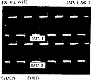 FIGURE D1 | 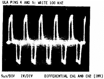 FIGURE D2 |
| MICRODRIVE SIGNAL (100 KHZ WRITE) | |
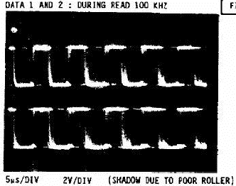 FIGURE D3 | 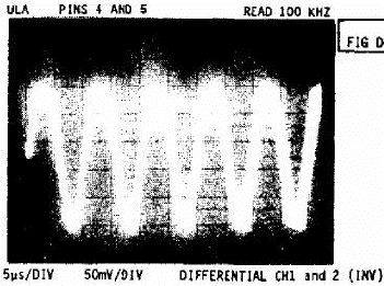 FIGURE D4 | 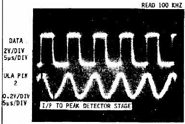 FIGURE D5 |
| MICRODRIVE SIGNALS (100 KHZ READ) | ||
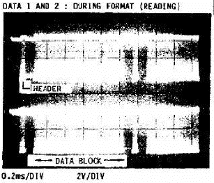 FIGURE D6 | 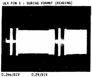 FIGURE D7 |  FIGURE D8 |
| MICRODRIVE SIGNALS (FORMAT READ) | ||
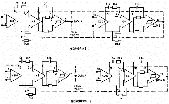
FIGURE D9 ULA 2G007 - INTERNAL CIRCUIT
| Previous | Contents | Next |
| System Test | Parts Lists |